Schematic Capture
Schematic Review
Component Creation
Netlist Importing
Mechanical DXF Importing
Placement
Placement Review
Component Verification and constraint setting
Routing
Routing Review
Gerber generation
Gerber Review
INPUT REQUIRED
Final Schematic
Final BOM with Part Number
Datasheets as per the P/N
Mechanical DXF or if any
Placement Constraint
Routing Constraint
Stack-up Details
OUTPUT DELIVERED
Design Files
Fabrication Files
Assembly Files
Stack-up File
Read-me File

Project Name : ESAFS
Number of Boards: 03
Project 01 : ESAFS-CPU Board
Number of Layers: 08
Project 02 : ESAFS-PWR Board
Number of Layers: 08
Project 03 : ESAFS-CONN Board
Number of Layers: 06
Microcontroller
RS422
SENSOR
Accelerometer
Power Supply

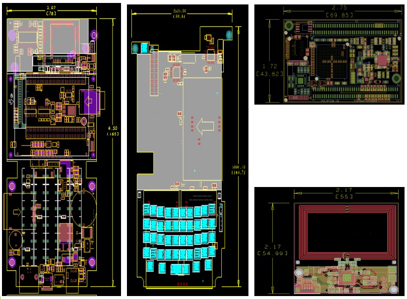
Project Name : TAB
Number of Boards : 06
Project 01 : Processor Board
Number of Layers: 08
Project 02 : GSM Board
Number of Layers: 04
Project 03 : Switch Board
Number of Layers: 02
Project 04 : Capsense Board
Number of Layers: 02
Project 05 : Connector Board
Number of Layers: 02
Project 06 : Connector Board
Number of Layers: 02

Project Name : RF EXTENDER
Number of Boards : 01
Number of Layers: 24
DSP
DDR3
NAND FLASH
SPI Interface
RF
EMMC
FPGA
Multiple Power Supply
Project Name : Ticket Issuing Machine
Number of Boards : 04
Project 01 : Main Board
Number of Layers: 06
Project 02 : SOM(System ON Module) Board
Number of Layers: 08
Project 03 : Antenna Board
Number of Layers: 04
Project 04 : Capsense Board
Number of Layers: 02

Project Name : Processor Board
Number of Boards: 01
Number of Layers: 06
Project Name : Digital Tele Protection Board
Number of Boards: 01
Number of Layers: 06
DSP Processor(TMS320C6211)
SDRAM Interface
SRAM Interface
CODEC Interface
DDR Interface
Power Supply
