Analog PCB Layout Design
Precision and excellence in analog PCB layout design. Differential Impedance signals routing and length matching are second habit for us, to ensure operational performance.
Digital PCB Layout Design
EMI/EMC constraints, DFM/DFT considerations, and clocking precision. We empower your digital circuits with PCB layouts that enhance performance and compliance for error free manufacturing.
Mixed Signal PCB Layout Design
Our expert team specializes in crafting layouts that seamlessly integrate complex circuitry, meeting your specific mixed-signal demands with precision and excellence.

About us
Company Overview
Gurudatta Design Services is a leading service provider in the field of PCB designing, located in Bangalore, India. Since its formation in the year 2020, it has been providing world-class quality services at the most competitive prices in the industry.
The experienced PCB Engineering team at Gurudatta Design Services works with clients across the globe addressing solutions for simple to highly complex PCB design solutions, which include high speed PCB design, RF design, High-Density Interconnect (HDI). The company also provides support for SI/ PI and thermal analysis, fabrication, and assembly by way of outsourcing.
We take pride in building long-lasting and trusted relationships with our clients and serve a wide range of clients which include large to small businesses and individuals. Our mission is to create value for our customers by providing exceptional quality service, error free designs and on time delivery.
PORTFOLIO
Here’s some of our products.
From a wide array of applications ranging from Smart Fan Control, Android Tablet, RFID scanner, PCIE and RF Extender, we have the skill and expertise to cater to your specific requirements.
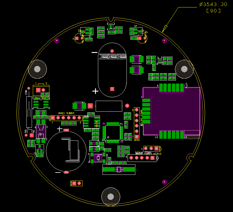
Project No. 1

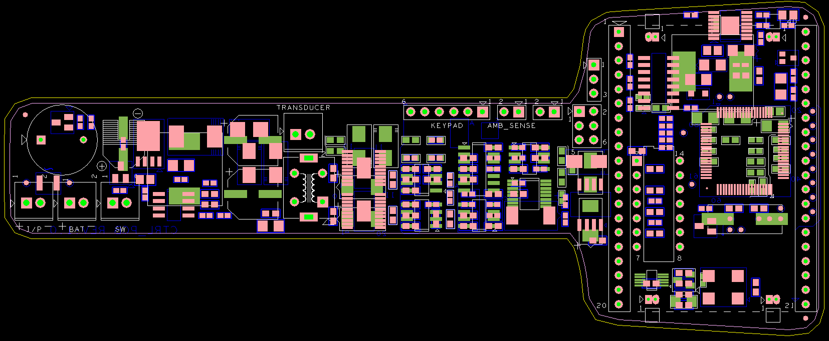
Project No. 2

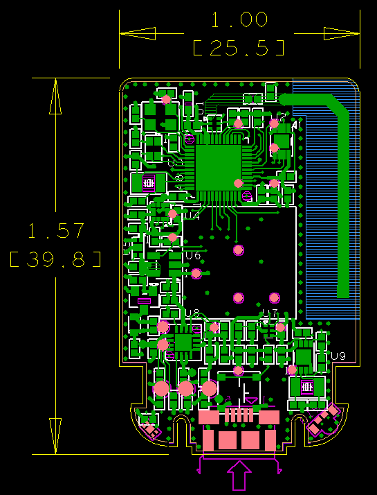
Project No. 3
Project No. 4
Latest news
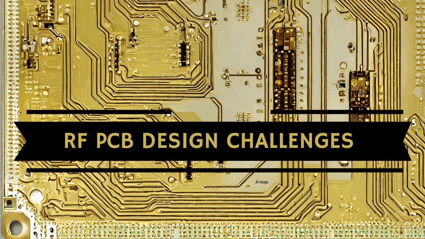
Challenges in Professional PCB RF Design – How to Overcome Them
Radio frequency (RF) PCB design is a complex and challenging field. Unlike[…]
